Page Contents
Hardware Design
Brief
The purpose of this project is to design, build a programmable guitar FX pedal using a Cortex-M4F micro and I2S. This will provide a platform for development and experimentation of DSP algorithms and techniques. This is also an experiment to use C++ in embedded development.
Evaluating the 24bit ADC and DAC
Digilent make a handy breakout board for a pair of 24bit ADC/DAC devices by Cirrus:

https://reference.digilentinc.com/reference/pmod/pmodi2s2/start
I chose the STM32F405 because it allows full duplex I2S, which means a single I2S peripheral can both send and receive. The pin connections between the ADC -> MCU -> DAC are shown below.
Note, the MCLK, LCRK, SCLK clock signals are electrically connected across both Cirrus devices and the MCU
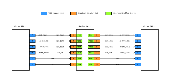
Using a Nucleo testboard I ran some quick test code to setup the peripherals. The signal integrity of the I2S device by passing in a sine wave and observing the output. The output met the specs of the Cirrus parts.
Prototype Design
System overview
One of the main features of a guitar pedal, other than the FX signal path, is the ability to bypass the FX signal path and route the signal to the output exactly as it came in. A relay is used to achieve this signal path routing and is controlled by a GPIO pin on the MCU. Several HW input switches and rotary encoders are connected to the GPIO pins of the MCU. These can be used to change parameters of the FX unit and are fully configurable depending on the need of the FX in use. An SDCard reader is also included to store data lookup tables for signal waveforms, filter coeffcients and other complex maths functions. FATFS will be used as the SDCard file system.
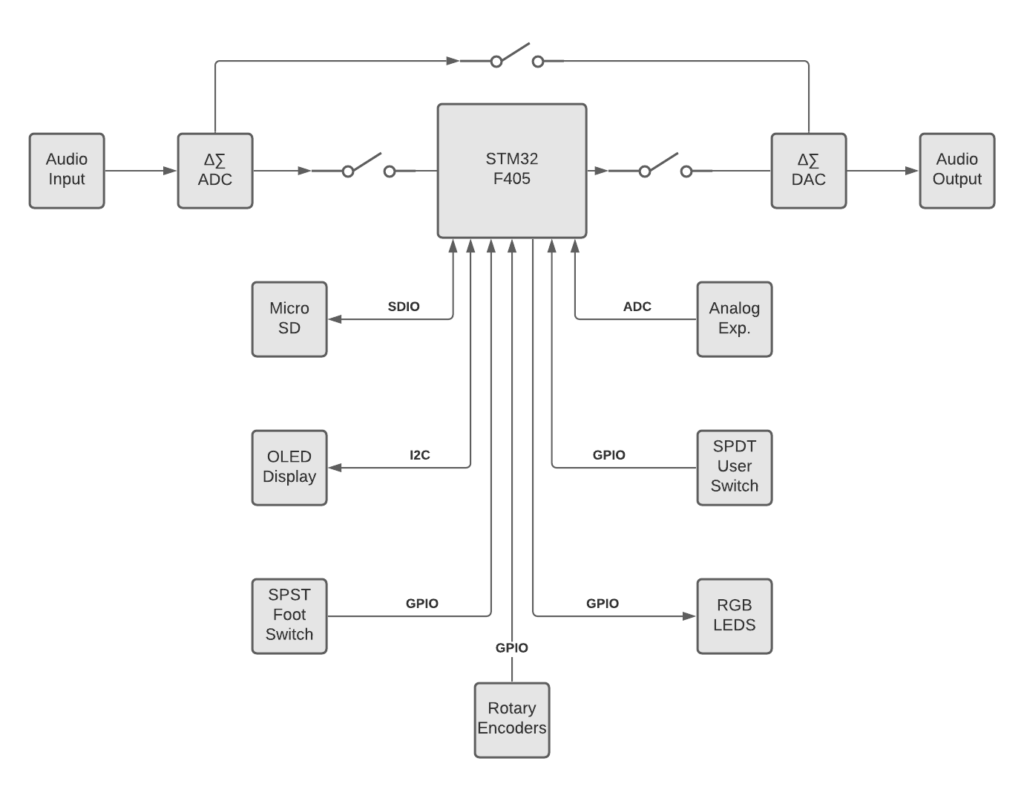
The analog input and output signals are conditioned using opamps. These serve a number of purposes:
1) High impedence input/Low impedeance output
2) Active filtering configuration (recommended by the ADC/DAC manufacturer.
3) Input volume control via a small potentiameter. This is not a user accessible input but can be used to adjust for different input gains according to application.
Dual voltage supply (+/-5V) for the OpAmps is achieved using a small TPS40600 charge pump IC.
Audio Input Schematic
Audio Output Schematic
MCU Schematic
The entire hardware project – containing the schematics – can be found here
Tools
I have used GNU 7-2018 with a JLink interface (SWD).
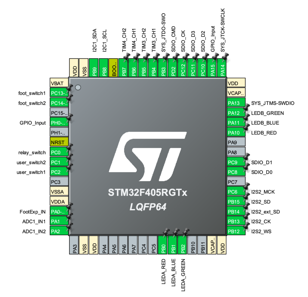
STM32CubeIDE provides a useful pin mux tool that can also be used to generate the startup code for the system. It has several advantages:
i) The configuration tool and code generator make it very quick to get started.
ii) I am very familiar with Eclipse-based IDEs.
ii) It is provided by the chip vendor, ST.
iii) It is free!.
Below is the pin assignment diagram:
Firmware Design
A class diagram for the system is shown below:
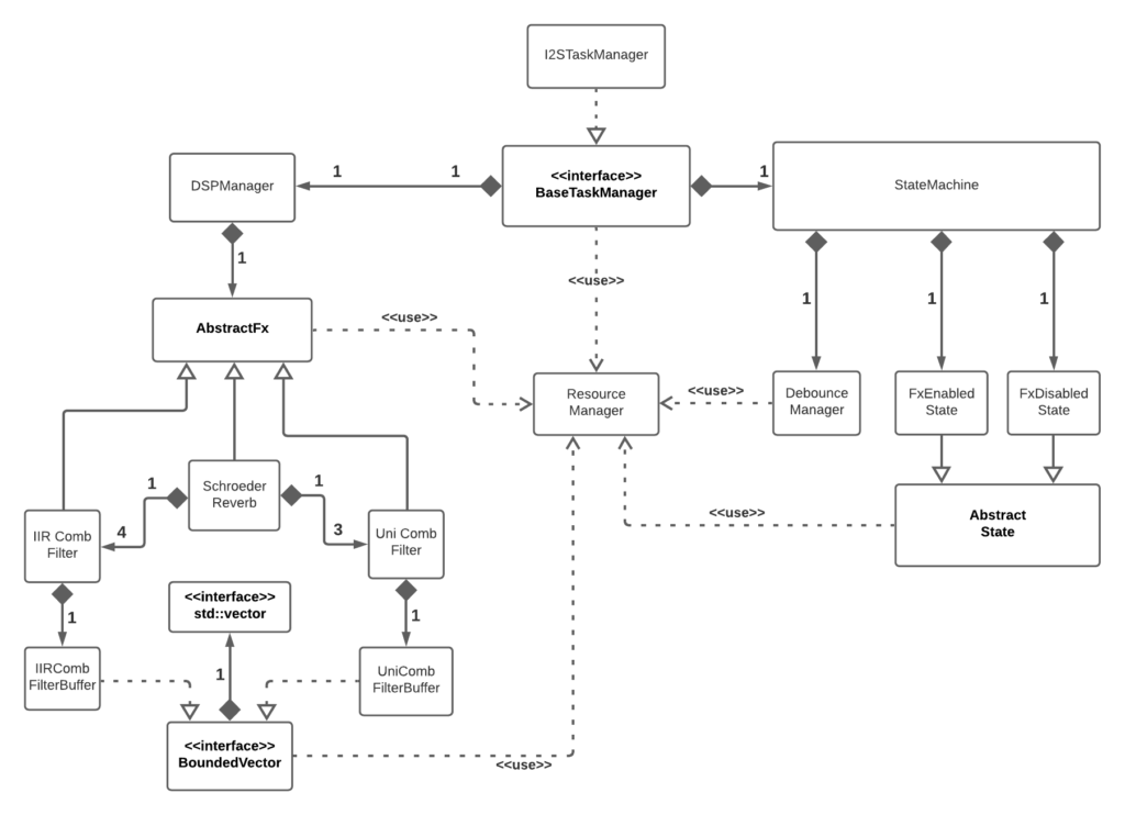
A State Machine tracks the system state and defines behaviour for incoming events. This follows the state pattern design where the behaviour is abstracted away from the state machine itself and into the individual states. The state machine retains the current state in the form of a pointer to a state object. When responding to a specific event, the state machine simply calls the event function belonging to that pointer, without knowing if the behaviour is correct or not.
A DPS Manager redirects the I2S data transferred from the I2S shift register into memory, and manage the digital signal processing algorithm. The effect is always stored as a pointer to AbstractFX, which allows the DPS Manager class to execute the DSP by simply calling the generic “process” function.
Resource Manager
A Resource Manager supervises the amount of memory allocated per call to operator new. Memory allocation on the heap is done only at system startup. Each class must have a local overloaded version of operatornew (std::nothrow). Calls to operatorneware forbidden. This has several purposes:
i) The memory allocation can be tracked during runtime.
ii) If the memory exceeds a set limit for the system, the allocation can be rejected.
iii) if the allocation is rejectednew (std::nothrow)is allowed to return anullptr. The application must be vigilent to check for nullptr return values and act accordingly.
iv) Operatornew is overloaded globally to identify any unauthorized memory allocations.
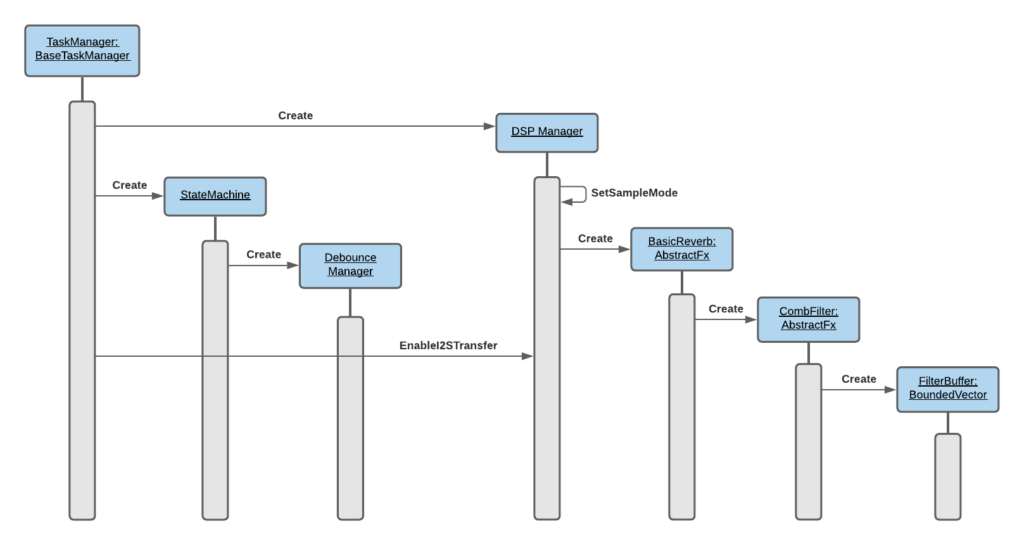
System start-up sequence diagram
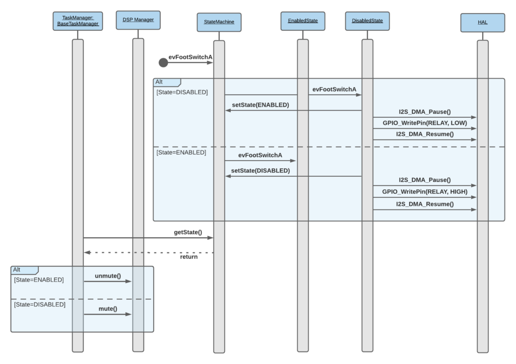
State machine sequence diagram
I2S data format
The Cirrus CS5343 24bit ADC and Cirrus CS4344 24bit DAC transmits/receives a 24bit packet in a 32bit frame over I2S serial. The left channel is sent first, followed by the right channel. Therefore to send both channels, two 32bit frames must be sent.
It’s important to note here that for both ADC/DAC and the STM32, the data is sent and received MSB first.

Since the STM32F405 only has a single 16bit register for receiving/transmitting I2S data, this must be done with two read/write operations using 16bit data values. The reference manual examples shows the value 0x8EAA33, the first packet must contain the first 16bits (0x8EAA) and the second packet must contain the last 8 bits plus 8 padding bits (0x33XX).

This means that each channel packet will consist of two unsigned 16bit integers, and the contents must be bitshifted to convert from I2S format to 32bit floating point format.
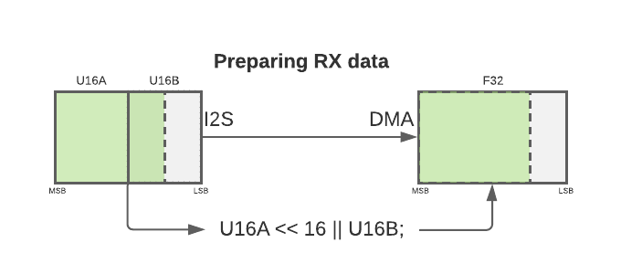
When receiving the data from the I2S Rx buffer, the first 16 must be left shifted 16 bits and bitwise OR’d with the second.
When tranmitting data to the I2S Tx buffer, the single 32bit float word is right shifted by 16 bits to put the 16 MSB into the first 16bit word, then a bitwise AND is used on the same 32bit float to mask only the 16 LSB for the second 16 bits.
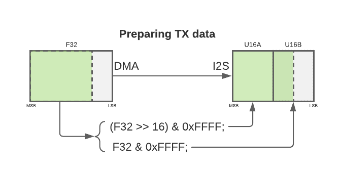
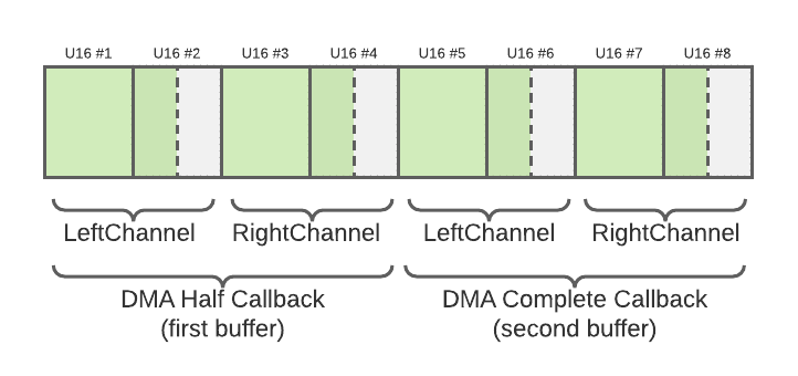
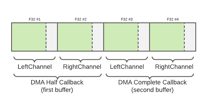
Using the STM32 DMA we can utilise the half and complete callback to double buffer the receive/transmit of data. Said another way, we can process one set of data while the other is being received/transmitted. Therefore, depending on whether the data is being sent into the I2S buffer or the DSP algorithm, the entire data can be represented as either;
1) two buffers comprised of a total 8 x U16 words:
2) two buffers comprised of a total 4 x F32 words:
The STM32 HAL provides convenient initialisation and callback functions. Naturally these API could be replaced and optimized. Although it is debatable how much overhead could be saved as the initalization is only done once at setup and the IRQ handler code used by the callback functions simply checks the various DMA status and error flags. Perhaps this code should be optimized as it has a bigger impact during run-time, but care should be taken not to skip these checks.
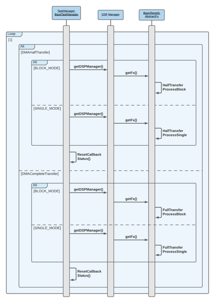
The DSP algrithm may prefer to receive its data in single or block mode (this will be covered in more detail later). Therefore two modes are available: SINGLE_SAMPLE_MODE and BLOCK_SAMPLE_MODE. The main difference is the DMA is setup to use either the two buffers comprised of a total 8 x U16 words, as shown above, or a multiple of this. Presently the multiple is set to 2048 but this can be easily modified. The benefits of either mode can be debatable: larger blocks can take longer to process but will require fewer interrupts. In practice your decision may be dictated by the DSP library. Writing single sample algorithms can be simpler but pre-existing libraries like CMSIS DSP use a sample block interface.
Given all the above information a sequence diagram is shown below. This shows the relationship between DMA transfer modes, sample modes, and the Task Manager, DSP Manager and AbstractFx classes.
Schroeder Reverb
Muting voltage spikes
When pressing the SPST footswitch, the coil relay redirects the signal path through the STM32F405. A brief voltage spike can be observed as the switching occurs. This lasts for about 2ms.
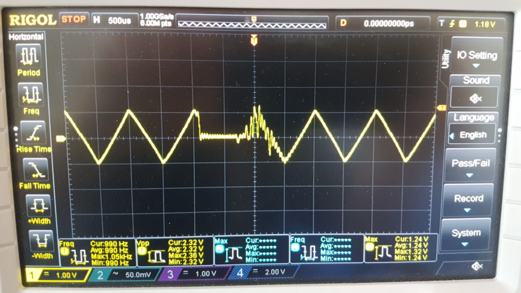
Whilst this is not always a problem, the spike is intensified by the reverb algorithm and the result is an echoing, crashing sound in the output.
How best to resolve this?
- Modify the hardware to prevent the spike from occurring.
- Further digital processing to soften the spike after it occurs.
- Mute the processing algorithm immediately after HW switch occurs for a short period.
All are valid solutions. Lets look at muting the algorithm.
Assuming max MCU clock frequency is 168MHz. One tick is 0.0059µs.
We know the duration of the spike is 2ms. Therefore we need mute the processing for:
2×10^-3 / 5.9×10^-9 = 338.9 ticks.
0.002 / 0.0000000059 = 338.9 ticks.
I added a third “mute” mode to the DSPManager, where no I2S data is handled.
When the state machine handles the foot switch event, the mute mode is enabled and a timer is started in “one pulse” mode. The callback for the timer disables mute mode, thereby restoring the signal after the timer period has elapsed.
Unfortunately, at best, this made no discernable difference. At worst, the added latency with the I2S data transfer caused error in the audio output.
Another idea in this area is to briefly disable the DMA transfer before changing the GPIO signal for the relay, before enabling the DMA transfer again.
void FxDisabledState::evFootswitchA(StateMachine *machine)
{
    if(machine == nullptr)
        error_handler();

    setState(machine, machine->theStateList[StateMachine::FX_ENABLED]);

    HAL_I2S_DMAPause(&hi2s2);
    HAL_GPIO_WritePin(RelayCoil_OUT_GPIO_Port, RelayCoil_OUT_Pin, GPIO_PIN_SET);
    HAL_I2S_DMAResume(&hi2s2);
}
Perhaps the circuit is flawed and needs re-examination:
When the N-channel FET is enabled with a GPIO high signal, the relay is enabled, and vice versa. There is a protection diode to prevent spikes damaging the rest of the circuit when the relay is powered off. However, maybe the diode is not suitable to cope with either speed or current of the relay. The coil resistance is HFD4/3 64.3Ω. At 3.3V, the current spike would be 5mA. The 1N4148 diode should be able to cope with this. It is also a fast small signal diode in the region of 4-8ns. So perhaps the diode is fine.
I could try adding a 1MΩ resistor on the input/output traces to ground. This could mitigate any large voltage spikes by shunting them to ground.
Improvements
- Onboard RAM for larger delay/reverb buffers
- Redesign the hardware signal path switching so that the ADC/MCU/DAC path can be completely bypassed. This would allow the DMA to be disabled/enabled and muted/re-synced when the signal is bypassed.
