Page Contents
DSP Peak Detector Algorithm
Note, X is the channel number.
MIXER_PEAK_MAPPING and SPLITTER_PEAK_MAPPING are used to support GPIO mappings for different PCB layouts.
ADC input demux
The data from multiple ADC channels is interlaced into a single array:
[0]=CH1, [1]=CH2, [2]=CH3, [3]=CH4, [5]=CH1...
This must be demuxed or binned according to ADC_NUMBER_OF_CHANS
Average sampled voltage signal
Software oversampling is used to reduce ADC input noise.
The ADC sample size is set by ADC_DATA_INDEX_SIZE_TOTAL which is split between ADC_NUMBER_OF_CHANS. Therefore, the number of samples per ADC channel is ADC_DATA_INDEX_SIZE_TOTAL / ADC_NUMBER_OF_CHANS
This is calculated in GetAverageAdcVolts().
The result is stored in adc_chX_avg_volts
Peak signal memory
The peak signal of adc_chX_avg_volts is stored in adc_chX_volts_peak.
If adc_chX_avg_volts is lesser than adc_chX_volts_peak then it is discarded.
Once a time window of RMS_MEM_LENGTH has expired, adc_chX_volts_peak is reset.
Peak signal threshold
If adc_chX_volts_peak is larger than adc_chX_volts_peak_threshold then the LED is set for channel X.
Peak signal release
The LED is reset periodically using a HW timer.
Therefore, the release period =
master_clock_freq / (timer_prescaler * timer_period)
PWM could be used for a smoother fade out, but care should be taken that the PWM frequency does not cause parasitic noise on the audio output.
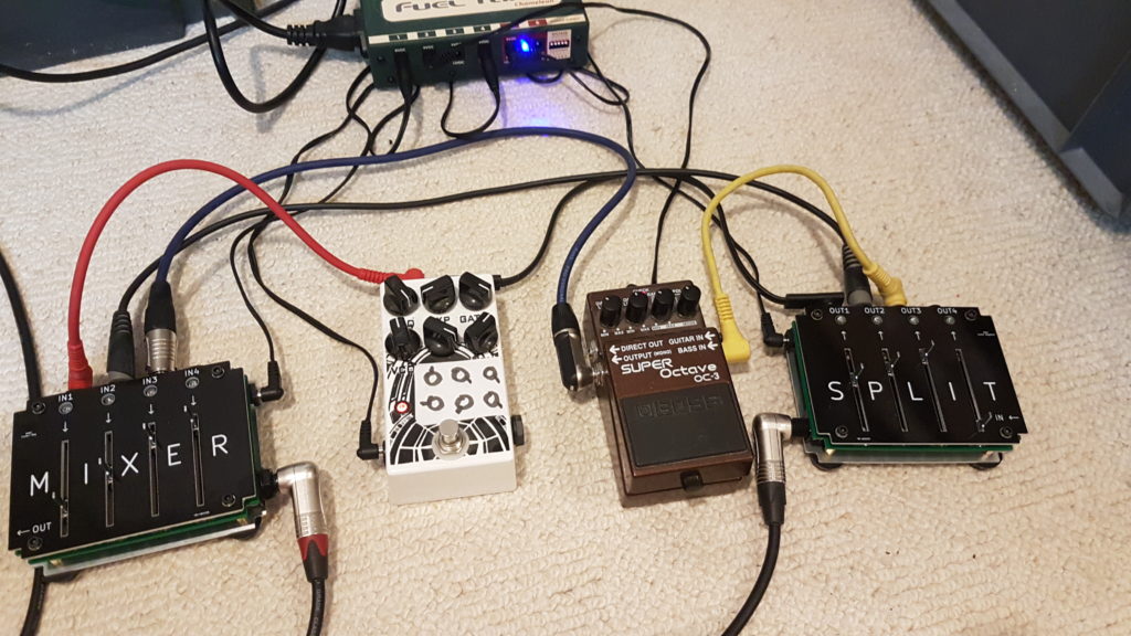
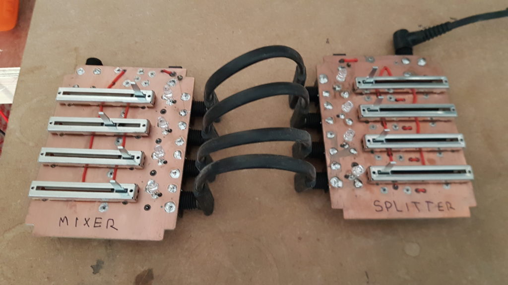
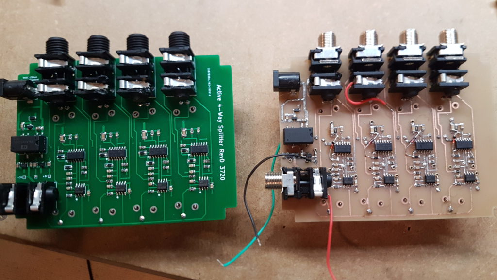
Active 4-way splitter pedal with digital peak detector
- Analog 1->4 splitter circuit with buffered input and output gain controls.
- Digital LED peak detector per output channel.
- Fits in a Hammond 1590BB enclosure (120mm x 95mm).
Required Kicad Hardware library: https://github.com/cracked-machine/KicadLibrary
Related SW project: https://github.com/cracked-machine/DigitalPeakDetector_SW
System Overview
Schematic
Top Level
Input Buffer and Gain Block
This uses a split supply op amp. The second stage is an inverting op amp configuration so that it can attenuate the input signal down to zero output.
Therefore the second op amp has very low input impedance and will cause “tone-suck” if used on its own. The solution is to add a preceding op amp stage in a non-inverting configuration that works as a high input impedance buffer.
Negative Rail Block
Each Input Buffer and Gain Block
MCU Peak Detector block
This section replaces the classic analog peak detector circuit with a microcontroller. The input signal is captured by the 12bit ADC of the microcontroller. The average input value and the output threshold are determined by software. When the output threshold is reached, the microcontroller briefly toggles the LED. The on/off time duration of the LED is also determined in software.
MCU Input Buffer block
This serves several purposes.
- It acts as a high impedance buffer and low pass filter for the ADC. This helps to provide a cleaner input signal for the ADC by removing high frequency noise.
- The 3.3V single supply of the op amp removes any parts of the input signal that swing above 3.3v and below ground (the limits of the microcontroller). In the event that a line level input signal was plugged into the input, the op amp would be damaged before the microcontroller.
Power Supply block
This linear regulator drops the 9VDC input to 3.3VDC. The power requirements of the system components are very low (~65mA) so the expected dissipation is also low (0.37W). A copper pad on both sides of the PCB (with connected vias) is provided to reduce this dissipation.
3D Renderings
PCB

Front Panel

Back Panel
This is the same back panel used for
ActiveMixerPedalWithDigitalPeakDetector_HW
PCB and panel profile
![]()
TODO
Some issues with the HW design:
- The PSU uses 3.3V for both MCU and Analog blocks. This is too low for the opamps in the analog blocks and does not allow enough headroom for the signal. This can result in clipping of the signal.
- The charge pumps used by the opamps in the analog blocks (used to create a negative voltage rail) need filtering. The negative voltage rail is noisy (observed on the scope) and a high pitched whine can be heard through the output when plugged into a large amplifier. A simple passive LPF would probably solve this.
- The input is on the wrong side!
Active 4-way mixer pedal with digital peak detector
- Analog 4->1 mixer circuit with buffered inputs and input gain control.
- Digital LED peak detector per input channel.
- Fits in a Hammond 1590BB enclosure (120mm x 95mm).
Required Kicad Hardware library: https://github.com/cracked-machine/KicadLibrary
Related SW project: https://github.com/cracked-machine/DigitalPeakDetector_SW
System Overview
Schematic
Top Level
Input Buffer and Gain Block
This uses a split supply op amp. The second stage is an inverting op amp configuration so that it can attenuate the input signal down to zero output.
Therefore the second op amp has very low input impedance and will cause “tone-suck” if used on its own. The solution is to add a preceding op amp stage in a non-inverting configuration that works as a high input impedance buffer.
Negative Rail Block
Each Input Buffer and Gain Block
MCU Peak Detector block
This section replaces the classic analog peak detector circuit with a microcontroller. The input signal is captured by the 12bit ADC of the microcontroller. The average input value and the output threshold are determined by software. When the output threshold is reached, the microcontroller briefly toggles the LED. The on/off time duration of the LED is also determined in software.
MCU Input Buffer block
This serves several purposes.
- It acts as a high impedance buffer and low pass filter for the ADC. This helps to provide a cleaner input signal for the ADC by removing high frequency noise.
- The 3.3V single supply of the op amp removes any parts of the input signal that swing above 3.3v and below ground (the limits of the microcontroller). In the event that a line level input signal was plugged into the input, the op amp would be damaged before the microcontroller.
Power Supply block
This linear regulator drops the 9VDC input to 3.3VDC. The power requirements of the system components are very low (~65mA) so the expected dissipation is also low (0.37W). A copper pad on both sides of the PCB (with connected vias) is provided to reduce this dissipation.
3D Renderings
PCB

Front Panel

Back Panel

PCB and panel profile
TODO
Some issues with the HW design:
- The PSU uses 3.3V for both MCU and Analog blocks. This is too low for the opamps in the analog blocks and does not allow enough headroom for the signal. This can result in clipping of the signal.
- The charge pumps used by the opamps in the analog blocks (used to create a negative voltage rail) need filtering. The negative voltage rail is noisy (observed on the scope) and a high pitched whine can be heard through the output when plugged into a large amplifier. A simple passive LPF would probably solve this.
- The output is on the wrong side!


