Ever needed a negative voltage rail to quickly test something on the bread board? Look no further.
- Abstract:
- Requirements:
- Schematic:
- PCB Layout:
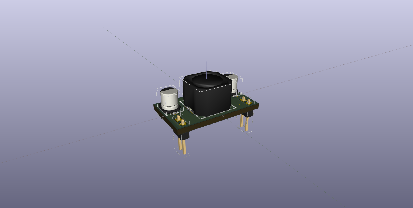
- 3D View:
Page Contents
This design uses the “classic” MC34063 switching regulator IC to invert the input voltage rail to a negative voltage, simultaneously stepping up/down the output depending on the position of the rotary dip switch. The resistors in this design are set for -3.3v, -5V, -9V and -15V.
The datasheet can be found here. Note that the maths to figure out the values looks horrendous but is actually not that bad. Depending on your requirements for ripple and noise the design has some tolerance for approximate values. Even still, a spreadsheet is recommended as usual!
The characteristics required and calculated results:
[embeddoc url=”http://bitshiftjo.cluster026.hosting.ovh.net/wp-content/uploads/2018/06/Breadboard_MC34063_InvertingRegulator_calculations2.xlsx” height=”600px” download=”all” viewer=”microsoft”]
For the curious few here are the formulas for the above calculations (taken from the MC34063 datasheet). You can also download the spreadsheet to see the details of my own calculations. Note, for this regulator design we are only interested in the inverting formulas (far right column).

The design follows the standard inverting configuration from the datasheet. The voltage divider at the bottom of the schematic – RDV1 and RDV2 – determines the output voltage. Originally I thought to use a simple SPDT 4-way DIP switch, but this IC configuration shorts when no selection i.e. no resistor, is present on pins 5 and 6. Since this IC has no thermal shutdown protection this should be avoided. Instead I opted for a CTS SERIES 220AD_10 rotary DIP switch so that a “not connected” selection is impossible. This switch has four selectable positions, doesn’t require BCD decoding (like many of the higher position switches) and also comes in both surface mount and through hole packages. Perfect for prototyping a PCB design on a breadboard!
Due to the size of the inductor and capacitors, these components are located on a different side to the other components.
Note that that pin headers needed to be exactly 23mm apart so that they would line up with the last but one column either side of the breadboard divider.


Just to be fancy, here are some 3D views of the proposed design.


